Bipolar Junction Transistor
The diode mental model
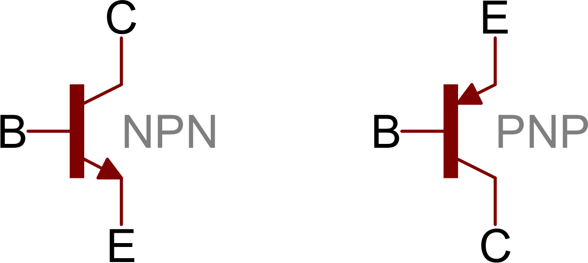
This style of transistor comes in two flavours: NPN and PNP. My preferred mental model for understanding the behaviour and differences of these two types of transistors is by focusing on the “diode” orientation. Although transistors are not diodes, nor do they contain one, they are similar enough that the diode symbol appears in the circuit symbols of BJTs:
In both cases, the arrow (the “diode”) shows which path the small base current flows on:
- The
NPNbase current flows from the base downwards to ground. Therefore there must be a high enough relative voltage on the base to overcome the diode voltage barrier and activate the transistor. - The
PNPbase current flows from the positive supply and out the base. Therefore there must be low enough relative voltage on the base to overcome the diode voltage barrier and activate the transistor.
Generally the relative voltage difference required to pass this barrier is 0.7 volts. Once this small current has been achieved, the transistor enters its active state and powers the load. In the diagram above I’m showing the load as a resister, but it could easily have been any analog device that requires high power such as a lightbulb.
Pin Names
- Base is the center pin, both physically and in the circuit diagram symbols, for both types of BJTs.
- Emitter is the right-most pin physically. In circuit diagrams, the “arrow” always connects the base to the emitter.
- Collector is the left-most pin physically. In circuit diagrams, this is the line that does not have an arrow, and is the side the load is attached to.
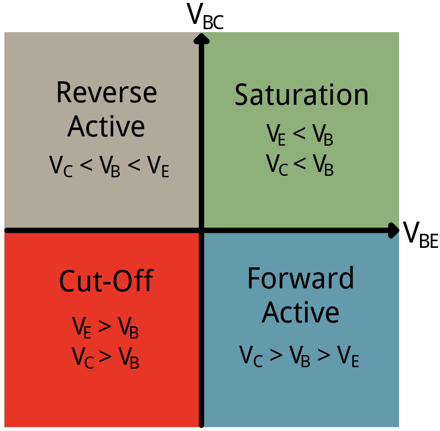
Modes of Operation
There are three main modes that a BJT can operate in: Cutoff, Active, and Saturation. Cutoff is the OFF (open circuit) state, Saturation is the ON (closed circuit) state, and Active exists as the transition between these two states.
The mode is determined by the relative voltages between the base-collector, and base-emitter. For an NPN transistor where the “diodes” only allow current to flow out of the base, these relative voltages would be as follows:
- Cutoff Mode:
Vb < Ve + 0.7ANDVb < Vc. In this mode no current flows from the collector to the emittor. - Active Mode:
Vb > Ve + 0.7ANDVb < Vc. In this mode the transistor acts like a variable resistor. As more current passes from the base to emittor, the lower the resistance between collector-emittor will be. This is a transition phase between the closed and open circuits. This mode is useful for building an amplifier circuit. - Saturation Mode:
Vb > Ve + 0.7ANDVb > Vc. In this mode the collector and emittor are effectively an open circuit.
Note: Remember that as current from the collector to emitter is increasing in active mode, the voltage on the collector pin is likely dropping (because more current through the resistor/load means a higher voltage drop). It is this voltage drop that will eventually make the condition of Vb > Vc (saturation mode) become true, not the voltage increase of Vb going higher and higher.
Reverse-Active Mode
There is a fourth mode of operation, although it is not a mode the BJT is exactly designed to operate in, it is helpful to know about to explain certain observed behaviours.
This mode acts similar to Active Mode, but the current is flowing in reverse. That is, a small current is flowing from base to collector and a proportial (amplified) current flows from emittor to collector. This mode occurrs when Vb > Vc and Vb < Ve
Note that this has the same effect as Active Mode in that it will tend towards Saturation as the base current increases. Therefore, if the base voltage is significantly higher than either collector or emittor (doesnt matter), the BJT will move to saturation
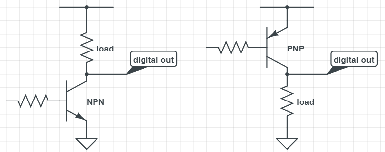
Load location & Digital Circuits
The location of the load on a BJT is important. To achieve a high impedence state on the load when the transistor is OFF, the load must be connected to the side opposite the diode. When the BJT is OFF, the load is receiving high impedence (an open circuit) from the transistor. When the BJT is ON, the load is short circuited to the other non-base pin.
In a digital circuit, using a resistor as the load is common because it can act as a pull-up or pull-down source for when the BJT is in its high impedence state. This is what the “digital out” shows in the above diagram.
In summary:
- An
NPNtransistor will drive low the digital out when base is relatively high, and pull high when base is low. - A
PNPtransistor will drive high the digital out when the base is relatively low, and pull low when the base is high.
The difference between driving and pulling is important in digital electronics. A bus can safely be pulled low and driven high simultaneously (the result is net high), but cannot be safely driven by two components at once (it may mean there is an effective short between 5v & GND, or end up in a uncertain 2.5v state).
For an example use, see BJT Tristate Digital Buffer.