BJT Tristate Digital Buffer
A tri-state digital buffer is a logic gate with two inputs and one output. It is used to selectively allow a signal to pass through to the output. The truth table is as follows (Z means high impedence, ie no value is driven):
| Enable (E) | Input (I) | Result (R) |
|---|---|---|
| 0 | 0 | Z |
| 0 | 1 | Z |
| 1 | 0 | 0 |
| 1 | 1 | 1 |
Example implementations using BJTs
Option 1: pull-down resistor on serial bus
In the below example we will make a design decision to only drive the result R to 5v when both E and I are high. We will assume that the result is a line we are comfortable having a pull-low resistor on, which will provide the 0v signal when E=1 & I=0. This is a reasonable design decision when the goal of using a tri-state buffer is primarily to ensure that nothing is being driven when E is low. This is useful when I is a device that is always trying to drive values onto a bus, and we want to force it to stop at certain times.
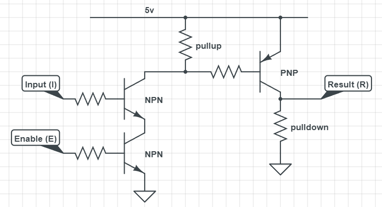
There are two stages to the above circuit:
EandIare put through an NAND gate constructed from two NPN transistors.- The PNP transistor drives the result
Rhigh only when the NAND gate delivers a low voltage to its base. In all other states, the result R is receiving high impedence from the PNP transistor, and will be pulled low.
Option 2: pull-up resistor on serial bus
This design is the same idea as the above design, but instead assumes that the result is a line we are comfortable having a pull-high resistor on. Therefore instead of driving the result to 5v, we will instead focus on driving the result to 0v when E=1 & I=0.
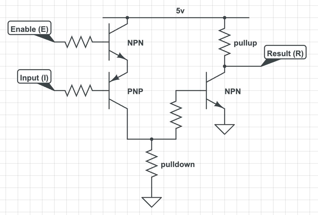
Again, there are two stages in this circuit:
- The first two BJTs perform the logic
E and (not I) - The right-most NPN transistor drives the result
Rlow only when the output of stage 1 istrue. In all other states of E & I, the result R is receiving high impedence from the BJT, and will be pulled high.