6502 Project
Below are some of the critical implementation details of my 6502 breadboard computer.
Parts Used
- CPU: W65C02S (modern version of 6502 which can hold state while clock is paused)
- EEPROM: AT28C256
- RAM: HM62256B
- Interface Adapter: W65C22
- LCD Driver: HD44780U
References
Address Map
0x0000 - 0x3FFF: RAM (Chip enabled on address{00** ****})0x4000 - 0x5FFF: Unused (Could expand RAM here by enabling on address{0[0*|10]** ****})0x6000 - 0x7FFF: I/O (Chip enabled on{011* ****})0x8000 - 0xFFFF: ROM (Chip enabled on{1*** ****})
Note: address range 0x0100 - 0x01FF is reserved for stack. The stack pointer register S stores the lower 8 bits, the 6502 is hard-coded to use 0x01 as the upper half.
Warning: The RAM timing does not work by directly connecting the address decode logic to the chip enable (CE) pin. Instead we need to only enable the chip while the clock is in its high state.
I/O Adapter
The lower four bits of the address bus are connected to the W65C22 interface adapter. Therefore the actual required address space for the LCD is 0x6000 - 0x600F.
LCD I/O
The I/O adapter has two ports: A and B. Port A drives the data pins of the LCD screen, while the lower three bits of port B drive the LCD flags (RS, R/W, and E)
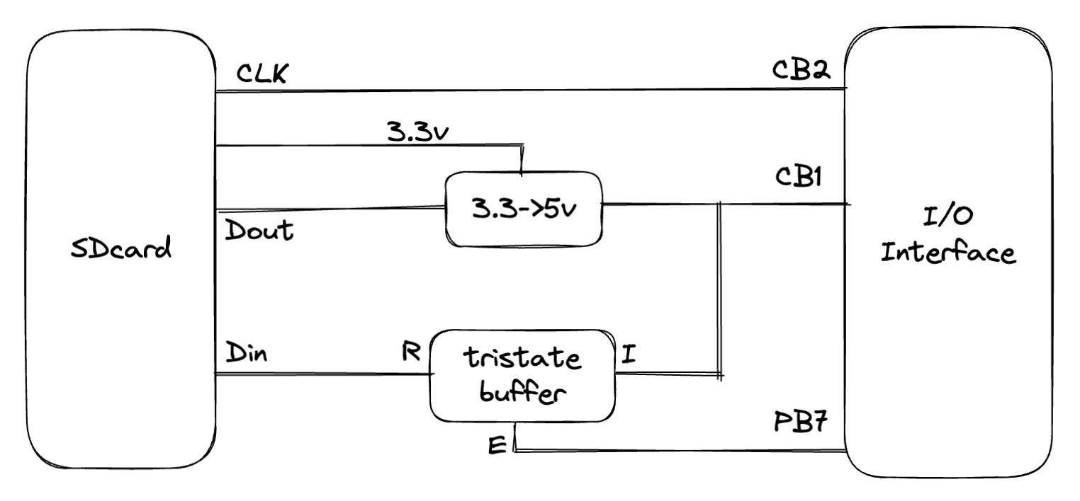
SD Card I/O
The SD card chip uses Serial Peripheral Interface (SPI) to communicate to the microcontroller. This standard has 3 main lines:
- CLK: the shared clock between the slave & master. Data is transferred on a rising clock signal
- MISO: Master-In-Slave-Out data line
- MOSI: Master-Out-Slace-In data line
To facilitate the serialization of bytes, I’m using the shift register in the W65C22. This feature provides the serialization, deserialization, and clock signal timing. However, there are two problems that I’ve had to address with additional hardware:
- Problem 1: The MISO line is only driven to 3.3v. To ensure the W65C22 is latching the correct values, I’m converting the 3.3v to 5v using a 3v to 5v level shifter.
- Problem 2: There is only one shift register in the W65C22 to share for input and output. Tying MISO and MOSI together directly does not quite work here because the SD card gets put into a bad state if we feed back its own output into its input. Therefore we need to disconnect the MOSI line from the serial bus when not in use. To facilitate this, I’m using a BJT Tristate Digital Buffer (the pullup version) with its enable
Einput connected to byte 7 (MSB) of the W65C22 PORT_B.
The resulting architecture:
Software Architecture Principles
- Based on the low amount of stack space: Subroutines do not guarantee register preservation, but do declare (via docs) which register state is voided. Callers may choose to push their registers to the stack before subroutines.